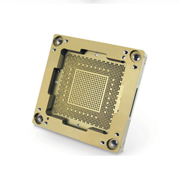
Product Overview
The Semiconductor Test Socket Guide is engineered to deliver consistent performance across thousands of test insertions. By controlling vertical axis movement, it prevents off-axis actuation that can cause uneven contact force or premature probe wear. Precision-machined guide holes with chamfered lead-ins and optimized clearance profiles ensure smooth compression of pogo pins. The result is repeatable contact resistance, extended socket life, and superior reliability in high-throughput ATE environments.
Surface & Finish
-
Contact Channels: Ra ≤ 0.2 µm (mirror finish)
-
Non-Contact Surfaces: Ra ≤ 0.8 µm
-
Burr-Free: Micro-deburred edges, ISO 13715 compliant
Protective Coatings & Plating Options
-
Hard-coat anodizing (Aluminum)
-
Electroless Nickel (50–100 µin)
-
Gold Flash (0.1–0.3 µin) for enhanced conductivity
Cleanliness & Packaging
-
Class 100 cleanroom packaging
-
Non-volatile residue <5 µg/cm²
-
Ion-free option available
Certifications
ISO 9001:2015 | IPC-9592 (High-Reliability) | MIL-STD-883
Technical Advantages
-
Built from CTE-matched polymers or ceramic-filled compounds for resistance to thermal distortion
-
Maintains dimensional stability at temperatures >150 °C during HTOL and burn-in procedures
-
Prevents warping, misalignment, or probe disengagement under thermal cycling
-
Designed for >100,000 insertions with high-hardness composites and abrasion-resistant materials
-
PTFE fillers or dry-film coatings reduce friction, galling, and particle generation
With its precision engineering, the Semiconductor Test Socket Guide ensures dimensional integrity, long-term durability, and reliable test results — even under demanding mechanical and thermal conditions.