Advanced Semiconductor Material Processing
Semiconductor materials such as silicon, gallium arsenide, and compound semiconductors demand exceptional precision during processing to preserve their electrical and thermal performance. These materials are widely used in high-performance applications where heat dissipation and structural reliability are critical. Through advanced precision machining, it is possible to create microstructures such as microchannels and vias that enhance thermal management and electrical conductivity.
Our expertise includes state-of-the-art techniques such as laser ablation, EDM, and micro-milling, enabling micro- to sub-micron level accuracy. This ensures that the intrinsic properties of the materials remain intact while meeting the rigorous performance and reliability requirements of next-generation semiconductor devices.
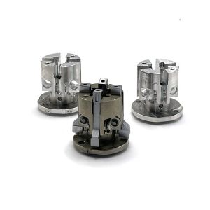
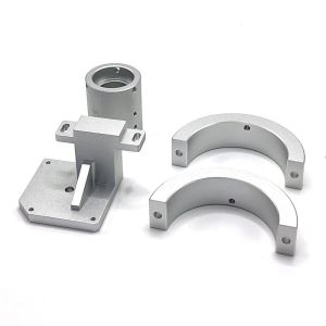
Our semiconductor inspection equipment components are manufactured through advanced CNC machining processes to deliver the highest levels of precision, consistency, and reliability required by the semiconductor industry. These critical parts are designed to withstand demanding testing environments, ensuring accuracy and stability in wafer inspection, probe stations, and other semiconductor testing systems.
Sub-Micron Precision You Can Trust
In semiconductor manufacturing, every micron matters. Tolerances as tight as 1–5 microns — and even beyond — are essential to ensure flawless device performance. Variations as small as wafer thickness or surface irregularities can reduce yield and compromise reliability.
Our advanced CNC systems, ultra-precision spindles, and real-time feedback technology enable consistent sub-micron accuracy. The result: components that fit perfectly, perform reliably, and meet the highest standards of next-generation semiconductor devices.
We work with a wide variety of high-performance materials such as stainless steel, aluminum alloys, tool steel, titanium, and engineering plastics (POM, PTFE, PEEK). With tolerance capabilities down to ±0.005mm, our machining process guarantees the exact fit and flawless functionality your applications demand.
To further enhance performance, we provide a full range of surface treatments including anodizing, electropolishing, nickel plating, passivation, and black oxide. Every component undergoes strict quality inspection using advanced measuring equipment such as CMM, surface roughness testers, and hardness testing machines. Full documentation, including material certificates, RoHS/REACH compliance, and COC, is available upon request.
Whether you need rapid prototyping, small batch production, or large-volume orders, our team can deliver high-quality semiconductor inspection parts with fast lead times and consistent results. All components are custom manufactured based on your 2D/3D CAD drawings and specific technical requirements.
✔ Ultra-High Precision CNC Machining
✔ Wide Range of Materials & Finishes
✔ Strict Quality Control & Certification
✔ OEM/ODM Support with Rapid Prototyping
✔ Reliable Packaging & Global Delivery